Part 1.0: Why even bother reading this blog post? What's the deal with silicon photonics?
There are a lot of great articles and textbooks explaining silicon photonics to the eager student or to professionals in adjacent industries. This is a post I wanted to write to instead explain silicon photonics to my mother, an accountant, or my father, an architect, or my wife, a software engineer. If reading the phrase "silicon photonics" conjures up images of Star Trek phasors or Las Vegas light shows, this is for you. My hope is that after reading this, you will have a more-than-vague sense of what silicon photonics is, but more importantly, have an idea of the wonderful opportunities that this technology enables. So read on, and set your phasors to stunningly down-to-earth descriptions of complex technologies.
As an academic, I have opened introductory sections of countless scientific research articles with, "Silicon photonics is a promising platform for..." or something close to it. I've always found this pattern a little odd. These articles are usually exclusively read by fellow peers within the scientific community researching the same thing as the authors and who are also experts within the field. The intended readers have dedicated years of their life to this subject just as the authors have. Here, though, I'm hoping to teach non-experts what silicon photonics is and why us researchers keep calling it a "promising platform."
The last decade and a half has shown that telecommunications products based on silicon photonics technology are both viable and lucrative. Companies such as Intel, Acacia (now Cisco), Luxtera (also now Cisco), and Elenion (now Nokia--is it too lame to name your own company?), and others have successfully brought to market various products and are shipping in volume. The central theses of these products is that you can get the performance out of silicon photonics to be "good enough" compared to conventional optical solutions that tended to have higher costs associated with them. Once the silicon photonics solution is "good enough," probably the cost of using it makes it a competitive offering in the market.
Beyond the currently-available products, there are a large number of potential applications the entire community is excited about. All of these opportunities can, quite frankly, revolutionize their respective industries. These applications include shrinking the size and cost of LIDAR chips so that every piece of machinery can accurately measure distance, put complex medical diagnostics right on your wrist, bring computers closer to human intelligence, bring quantum computers into reality, or even just make those augmented reality glasses useful and actually magical.
The trick with each of those revolutionary things is they all have two things in common: (1) The manipulation of light in incredibly precise ways and (2) the benefit from being able to put lots of things that can control light in precise ways all next to each other in large quantities. So, naturally, the first thing to know about silicon photonics is that it's a technology that is incredibly suited to manipulate light in precise ways--sometimes even individual photons. Thus, the use of the word "photonics" to describe the category of science the field falls into. To understand all the neat applications of silicon photonics technology, it's necessary to understand the meaning of that second point. That's where the "silicon" comes into play. The next blog post in this series will dive back into those revolutionary possibilities in more detail. But first, an abridged science lesson in silicon.
Part 1.1: Dissecting a phrase: The "silicon" in silicon photonics
The word "silicon" in "silicon photonics" really is half of the reason it is such a hot area of research. The computer chip industry, more formally called the "semiconductor industry," has long focused on using silicon as the starting material for manufacturing computer chips. Understanding what silicon is and why it is used is critical to understanding silicon photonics.
There are gigantic tomes, textbooks, nonfiction & fiction books, and academic literature all explaining what silicon, the element and material used in the semiconductor industry, is. For now, the few key points we'll discuss in brief here are: (1) silicon isn't the same thing as silicone, (2) material properties of silicon made it ideal for manufacturing computer chips, and (3) because of how ideal silicon is for computer chip manufacturing, a huge amount of money has been poured into the surrounding manufacturing infrastructure. This is good news for anyone that wants to use silicon computer chip manufacturing technology to do more than just make computer chips.
Part 1.2: Silicon isn't the same thing as silicone.
Silicon is an element on the periodic table, like hydrogen, oxygen, carbon, uranium, einstenium, and so on. If you are careful (this is an understatement), silicon will form into a crystal, similar to how carbon atoms will form into a diamond crystal that you might wear on your finger. Silicone, on the other hand, is a rubbery material made out of many different elements, including silicon.
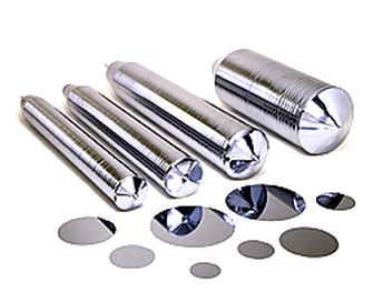
Silicon is one of the most abundant elements on the planet, existing in some form in the sand on the beach or, more significantly, comprising 30% of the earth's crust. Most of the silicon used in the semiconductor industry is mined from high purity quartz deposits, such as in Spruce Pine, North Carolina. The silicon mined from these quartz deposits is eventually purified to get to 99.999999999% or even 99.99999999999% purity (that's 11 nines, or 1 non-silicon atom per 100 billion silicon atoms). The highly purified silicon is formed into a long cylindrical single crystal and then that cylinder of crystalline silicon is sliced into individual discs called "wafers" and polished to nearly atomic flatness.
Why am I telling you what crystalline silicon looks like? I think understanding the manufacturing process steps for silicon-based chips is helpful to understand the promise of silicon photonics. Having a vision of high-purity silicon wafers getting printed with electronic circuits is helpful to later understand how the silicon photonics world reused all of this silicon manufacturing infrastructure to build photonic circuits instead of electrical circuits. (I will explain what a "photonic circuit" is later in this blog).
So now we have this super flat and super high-purity disc of silicon. Then what? These silicon wafers are the starting material for most of the computer chips you see around you. Electrical circuits are patterned onto the wafers by adding other materials on top of the wafers, such as insulating glass, conducting metals like copper, and intentional impurities to craft circuits with the desired properties.
"Patterning" electrical circuits is exactly as it sounds. For each layer of material that is added or subtracted there is a stencil pattern defining the area that has material added or subtracted. The stencils, or "masks," themselves aren't used to directly to add material like you might use a stencil to trace a picture with a pencil. Instead, a liquid material that is sensitive to light is coated onto the wafers. Light is shone through the stencils onto this liquid that is coated on the silicon wafers, solidifying the liquid and allowing part of it to be washed away, depending on where the stencil pattern let light through.
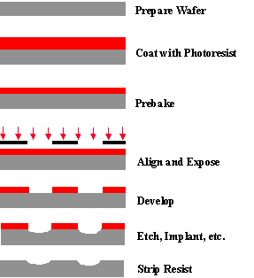
If metal wires are being added to the wafers, then metal is added everywhere, including both on the remaining polymer and on the silicon wafers. An acid is used to remove the polymer, taking off the metal that was added on top, leaving metal only where the stencil pattern dictated. Similarly, if material is being removed, it will only be removed where the polymer isn't. There are even more complicated ways to use this process to define shapes where material is added or subtracted, but this is the key image to have. We can take silicon wafers, and build up layers of incredibly complex electrical wiring and circuits. But why silicon in the first place?
Part 1.2: Material properties of silicon made it ideal for manufacturing computer chips
In principle, this kind of additive manufacturing can be performed on other materials, like crystalline germanium, gallium arsenide, and other exotic sounding things. In fact, all of these other materials are also used to make parts of specialized computer chips. However, the vast majority of chips manufactured are primarily made out of silicon. The technology to manufacture circuits all next to each other on a single layer ("a planar process") was key to making computer chips. Key to enabling that manufacturability is the inherent property of silicon that allows the growth of super high quality layers of glass on top of silicon in incredibly precise ways. The latest silicon manufacturing processes grow layers of glass in thicknesses of single-digit number of atoms.
It's hard to overstate just how magical this property of silicon to grow a super-pure layer of glass is. There are many ways to do it, but essentially the wafer is baked at some high temperature, such as 800°C (about 1500°F), and exposed to either air (O2) or water (H2O), and glass (SiO2) starts appearing on the surface. There is sort of a logical jump from "really nice layers of glass" to "working computer chip," but the key thing is the first part: really nice layers of glass. With that material property of silicon, engineers were able to figure out the rest: adding bits of metal and other materials to make electrical circuits. With enough electrical circuits all on the same chip, engineers eventually came up with "computer chips."
Silicon, in general, isn't the best possible device to make electrical circuits. Gallium arsenide, germanium, indium phosphide, and many other materials allow for better on-chip electrical devices (namely, transistors). Silicon is the dominant technology for computer chip manufacturing because it has the best economics. This ability to create a uniform layer of glass, and the ensuing designs based around transistors created this way, meant that electrical circuits with hundreds, then thousands, then millions, and now billions of individual devices could be made reliably on a silicon wafer.
Up to now, I've been freely using the phrase "computer chips" without really explaining what a chip is or that not all of these chips are actually used in computers, specifically. It was just handy to call them computer chips because this is something at least most people are familiar with. A chip is usually a piece of the silicon wafer containing a circuit that has been cut out. For use in things like your laptop or cell phone, a company will take this chip from the silicon wafer and "package it," meaning they will connect to it electrically and put it in some sort of larger protective case or material. Confusingly, this is also referred to as a "chip" within the industry. To help distinguish between the bare piece of silicon and the packaged piece of silicon, we usually call the bare piece of silicon, cut out and separated from a whole wafer, a silicon "die."
Part 1.3: Because of how ideal silicon is for computer chip manufacturing, a huge amount of money has been poured into the surrounding manufacturing infrastructure. This is good news for anyone that wants to use silicon computer chip manufacturing technology to do more than just make computer chips.
The number of individual transistors per chip has gone from thousands to millions to now tens of billions. In part, this is because large efforts have been made to shrink the size of a transistor so more of them can fit on a single chip. Additionally, the repeatability with which it is possible to manufacture transistors on a computer chip has improved. It's no use having a billion transistors if a few million of them don't come out the way you want them to.
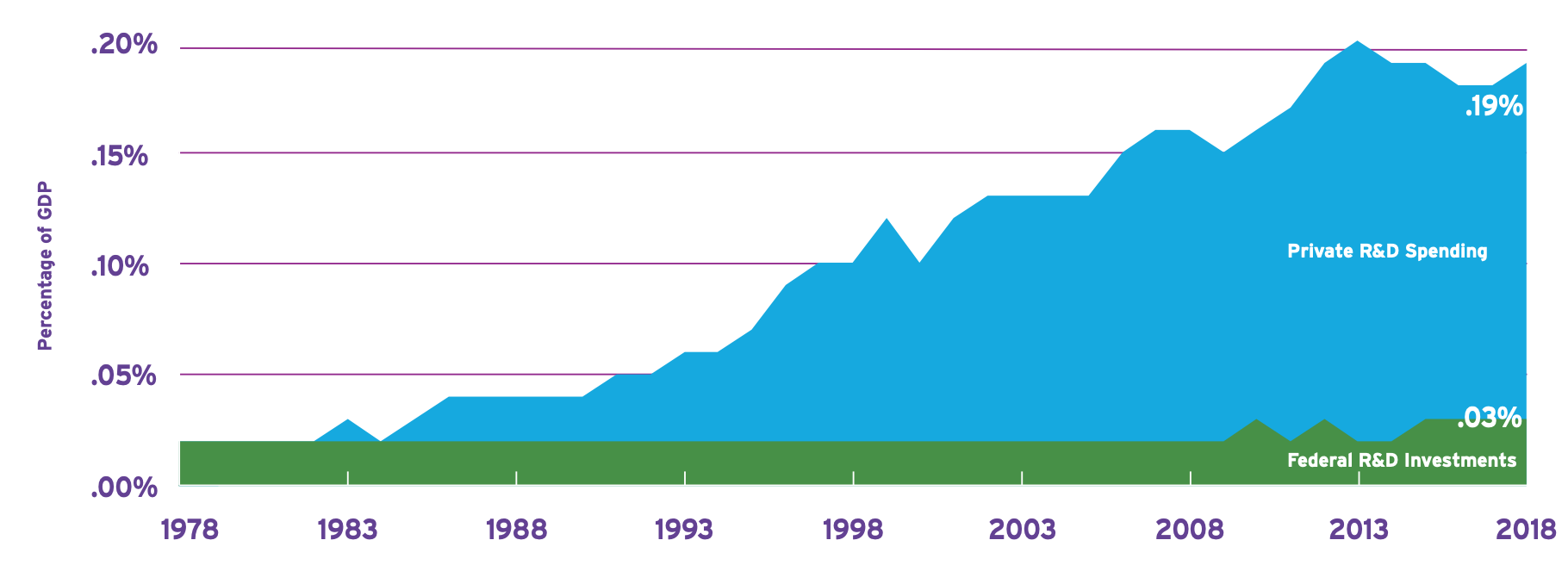
The latest-and-greatest manufacturing facilities cost ten or multiple tens of billions of dollars to construct. Though, looking at the cost of a single latest-and-greatest manufacturing facility (colloquially, called a "fab" within the industry), understates the decades of cumulative investment into the manufacturing equipment that each one of those fabs must purchase. For example, in 2019 one of the top equipment companies, ASML, alone spent $2.2 billion in R&D. In that same year an estimated $770 million was invested into R&D by various companies improving things like vacuum pumps, valves, heat exchangers, power supplies, and other critical manufacturing subsystems mostly just for the sake of making equipment to make computer chips. Leading into the present day, the investment has been steadily growing over decades.
One caveat to looking at the manufacturing R&D is that not all new technologies require cutting-edge manufacturing. Often, the fabs and tools inside those fabs built a decade or two ago are still good enough for many different applications, including the unglamorous act of continuing to manufacture older chips. The difference between the latest-and-greatest fabs and older generations of fabs often come down to how small of a feature the technology requires. There are, of course, other nuances, but the smallest feature of the chips being manufactured is a large driver of how advanced the manufacturing needs to be. Using "old" manufacturing technology can also be an advantage: the processing is typically very well-controlled and using these processes can be relatively cheap.
Part 1.4: Dissecting a phrase: The "photonics" in "silicon photonics" is probably a more unfamiliar word than silicon was. But also, "photonics" is half of "silicon photonics" and perhaps you are already tired of reading.
You've probably at least heard the phrase "silicon valley," and so when I use the word "silicon" you may imagine a series of technology giants' glassy buildings basking in the sunshine of northern California. Perhaps photonics has a shakier root in your mind. Photonics is a field of science relating to light (photonics --> photon --> light). We use "photonics" instead of "optics" when we want to sound more impressive and convey a general sense that we might be dealing with more of the physics of how light fundamentally "works," as opposed to "optics" where we might manipulate light like with a lens in your camera.
The thousand-page tome Fundamentals of Photonics by professors Saleh and Teich prefaces that the term photonics became commonplace in the early 1990s and that "the field was characterized by a collection of appellations that were not always clearly delineated...." and goes on to specifically define photonics as being "understood to include topics that rely on the interaction of light and matter, and is dedicated to the study of devices and systems." So I think we can get into what photonics means by looking at examples of what a photonic device or photonic system are.
Photonic devices take on many forms. The LED lighting in your work and homes was once a photonic device research project. Same goes for the LCD display in your car, or the image sensors in your camera, or the fiber optic cables that carry your internet, or the multitude of devices in the path of that fiber optic cable that encode information onto light and detect it. Meanwhile, photonic systems are assemblies of these devices. For example, a photonic communication system might include a laser to generate light, an optical fiber to carry it across great distances, an optical amplifier to make the light brighter, and a photodetector to convert the light into an electrical signal.
Silicon photonics gets interesting when we talk about systems. Just like in the electronics world, silicon, as a material, is generally worse at most optical functions than other materials--no light source, slower devices to switch light, and slower devices to detect light. The advantages come when we start looking at photonic systems built with silicon. In Part 2 of this blog post, I'll walk through just how we're able to build complex photonic systems in silicon.